High- Mobility Graphene
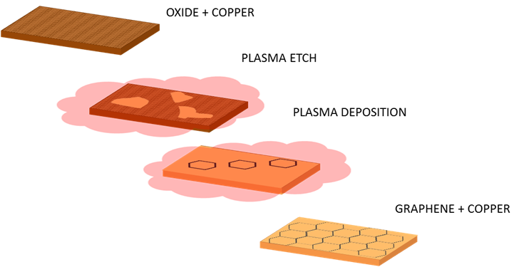
Schematic of the graphene deposition process
Current methods of chemical vapor deposition (CVD) of graphene on copper are complicated by multiple processing steps and by high temperatures required in both preparing the copper and inducing subsequent film growth. We recently demonstrated a plasma-enhanced CVD chemistry that enables the entire process to take place in a single step, at reduced temperatures (< 420 degrees Celsius), and in a matter of minutes.
Growth on copper foils is found to nucleate from arrays of well-aligned domains that coalesce into a nearly seamless films. These graphene films possess sub-nanometer smoothness, excellent crystalline quality, low strain, few defects and room temperature electrical mobility that is better than that of large, single-crystalline graphene derived from thermal CVD growth.
These results indicate that elevated temperatures and crystalline substrates are not necessary for synthesizing high-quality graphene.